1.2 What is being built: PCB vs PCBA vs box build
Precision in engineering terminology prevents significant manufacturing delays. Conflating the term “PCB” with “PCBA” confuses supply chains, invalidates vendor quotes, and creates unnecessary costs. The manufacturing process builds in stages: the bare board is a component of the assembly, and the assembly itself becomes a component of the final system. Clearly understanding the physical scope of the product is essential to effectively control cost, schedule, and quality at each tier.
1. PCB (Printed Circuit Board)
Section titled “1. PCB (Printed Circuit Board)”Definition: The bare board. It serves as both the mechanical chassis and the electrical highway for the circuit, consisting of a non-conductive substrate (such as FR4) and conductive copper traces. At this stage, it contains no electronic components.
The engineering reality
Section titled “The engineering reality”It is best to treat the PCB as a complex, custom-engineered mechanical part, rather than a generic commodity. Its creation requires intricate chemical etching, precision drilling, and multi-stage plating. Once the board is fabricated, its physical structure is permanently set.
The Risk: Should the PCB design contain a layout error, any subsequent assembly built on that board will either fail or require expensive manual rework, such as cutting traces or adding jumper wires.
- Suppliers: Dedicated PCB Fabrication Houses (Fab Houses).
- Key Tooling: Electrical test (E-test) fixtures, silkscreen screens.
- Typical Defects: Open circuits, shorts, trace delamination, warped boards.
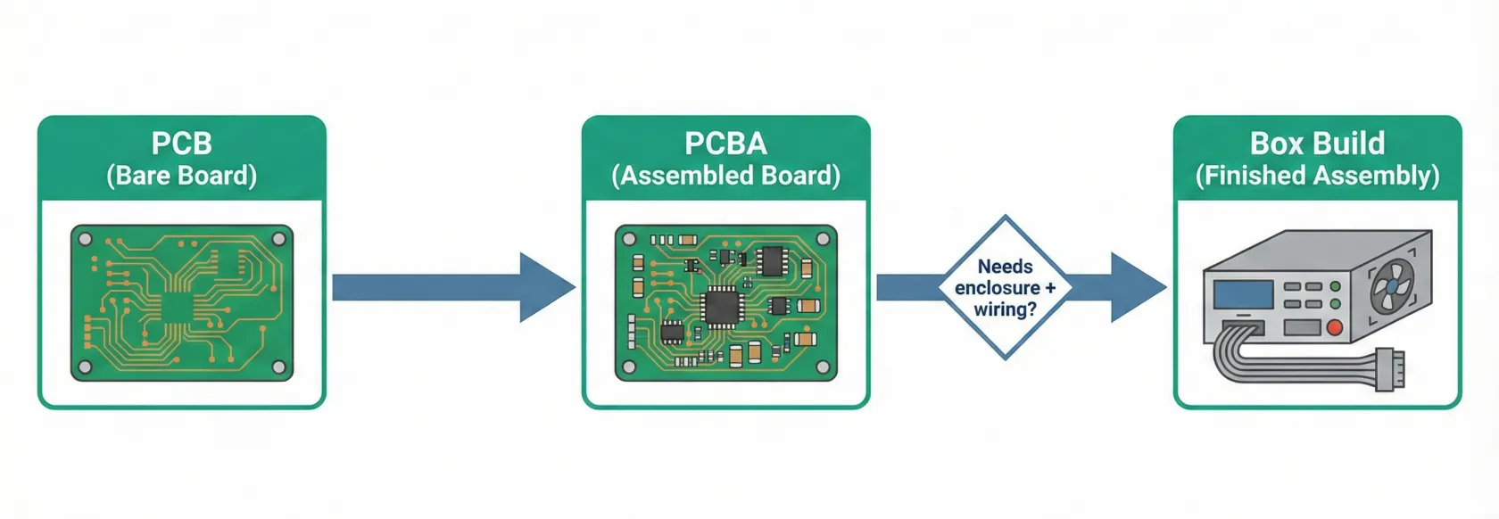
2. PCBA (Printed Circuit Board Assembly)
Section titled “2. PCBA (Printed Circuit Board Assembly)”Definition: The functional engine of the device. This is the result of soldering electronic components onto the bare PCB. This critical step transforms the passive board into an active, functional electronic device.
The engineering reality
Section titled “The engineering reality”This stage introduces complex thermal dynamics and chemical reactions, such as flux activation. The ultimate goal of the SMT line is to create thousands of reliable intermetallic bonds simultaneously across the entire board.
The Risk: Whenever the thermal profile of the reflow oven is incorrect, the resulting solder joints can become cold and brittle, or the sensitive components might be permanently damaged by excess heat.
- Suppliers: EMS Providers (Assembly Lines).
- Key Tooling: Solder stencils, Pick & Place programs, reflow profiles, ICT (In-Circuit Testing) fixtures.
- Typical Defects: Solder bridges, tombstoned components, missing parts, reversed polarity.
3. Box build (system integration)
Section titled “3. Box build (system integration)”Definition: The finished, enclosed product. This stage integrates the working PCBA into a final enclosure alongside human-machine interfaces, wire harnesses, and final retail packaging. It is now completely ready for the end-user.
The engineering reality
Section titled “The engineering reality”At this stage, the process moves away from automated, microscopic precision and leans heavily on manual mechanical assembly. The primary focus shifts from microscopic solder defects to macroscopic issues regarding physical fit and overall system function.
The Risk: Misaligned mechanical tolerances result in the PCBA failing to fit inside the enclosure, or external connectors failing to align properly with the chassis ports.
- Suppliers: EMS Providers (System Assembly Departments) or dedicated Contract Manufacturers.
- Key Tooling: Injection molds, assembly jigs, functional test stands, screw-driving robots.
- Typical Defects: Cosmetic scratches, pinched internal cables, loose fasteners, firmware version mismatches.
Cost and complexity scaling
Section titled “Cost and complexity scaling”Moving from a bare PCB to a complete Box Build greatly increases the number of variables that require active management.
Cost considerations
Section titled “Cost considerations”- PCB: Material cost plus Fabrication labor (generally a low unit cost).
- PCBA: PCB + Components (which often make up 80% of the entire BOM cost) + Assembly Labor and Machine Time.
- Box Build: PCBA + Mechanical parts + Manual Labor + Logistics. Shipping fully assembled, bulky units significantly increases freight costs due to volumetric weight.
Lead time factors
Section titled “Lead time factors”- PCB: Typically a 1–3 weeks standard fabrication time.
- PCBA: Dictated by the longest lead-time item on the BOM. A single critical IC requiring a 40-week delivery cycle forces the entire PCBA schedule to match that duration.
- Box Build: Inherits the PCBA lead time but also includes mechanical tooling lead times. For example, cutting steel molds for customized plastic cases can easily take anywhere from 8 to 12 weeks.
Recap: PCB vs PCBA vs Box Build Manufacturing Stages
Section titled “Recap: PCB vs PCBA vs Box Build Manufacturing Stages”| Stage | Primary Risk | Critical Control | Key Tooling |
|---|---|---|---|
| PCB | Layout error causing assembly failure | No opens, shorts, or delamination; permanent structure | Electrical test fixtures, silkscreen screens |
| PCBA | Incorrect thermal profile causing brittle joints or component damage | Solder joint integrity; requires verification beyond visual inspection | Solder stencils, AOI, X-ray, ICT fixtures, reflow profiles |
| Box Build | Misaligned mechanical tolerances preventing fit or function | Physical fit, connector alignment, overall system function | Assembly jigs, functional test stands, injection molds |